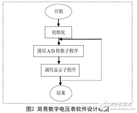
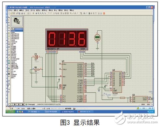
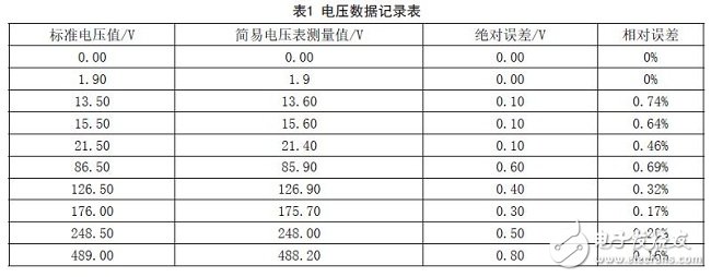
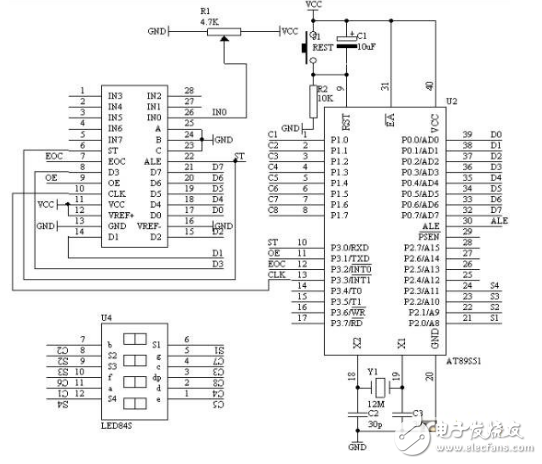
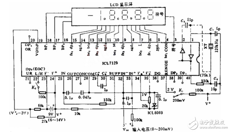
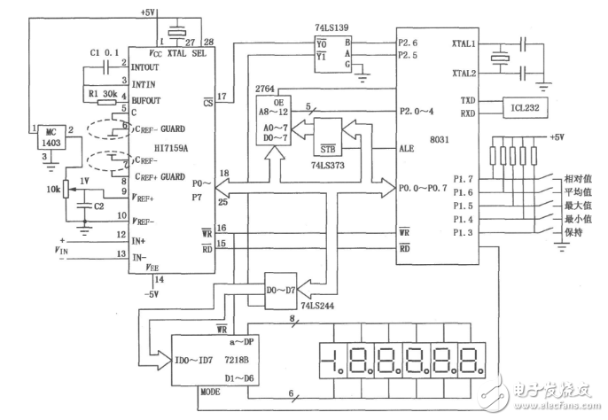
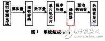
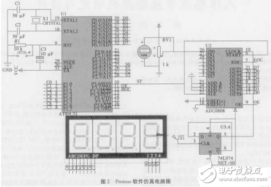
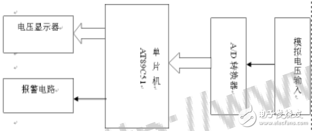
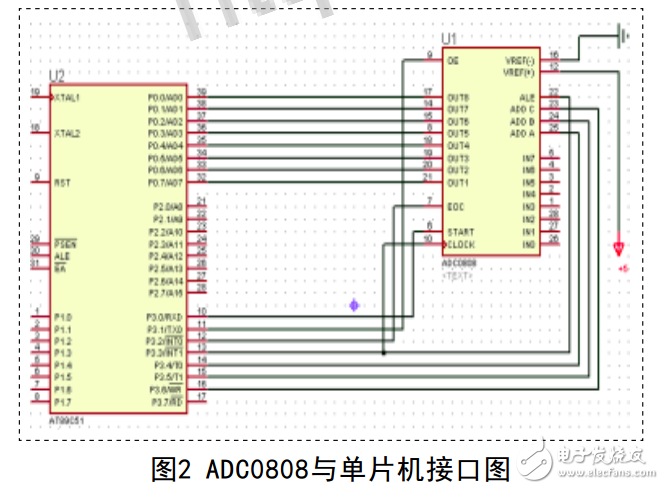
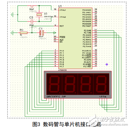
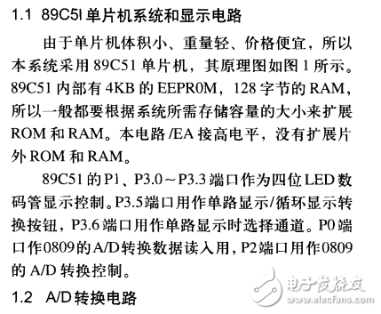
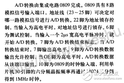
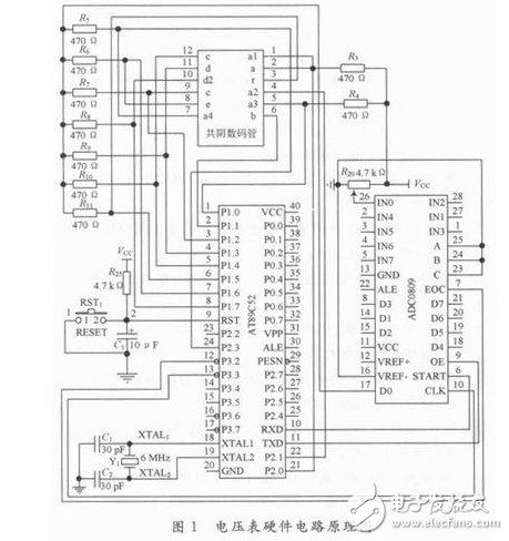
In the measurement of electricity, voltage, current and frequency are the most basic three measurements, and the voltage measurement is the most common. Now the digital multimeter used by students can measure a variety of power, and has a certain precision and is easy to use. In order to let students better understand the working principle of digital voltmeters and stimulate their interest in MCU courses, this paper starts with software and hardware design, proteus simulation, production of real objects, error analysis, and explains how digital voltmeter works. , data processing method, digital signal software filtering principle. The hardware circuit design consists of four parts: a/d conversion circuit, at89c51 single-chip system, led display system, and measurement voltage input circuit. The hardware circuit design block diagram is shown as in Fig. 1. The overall design block diagram is as follows: The working principle of this circuit is: +5v analog voltage signal is divided by the in0 channel of adc08008 after being divided by the varistor vr1 (due to the in0 channel used, so adda, addb, addc are connected to low level), after analog/digital conversion The corresponding digital quantity is transmitted to the p0 port of the at89c51 chip through its output channel d0-d7, and the at89c51 is responsible for processing the received digital quantity through the data, and generating the correct 7-segment digital tube display segment code to be transmitted to the four-digit led. At the same time, it also controls the digital tube to turn on and off through its four-bit i/o port p2.0, p2.1, p2.2, p2.3. The hardware circuit of the simple digital DC voltmeter has been designed, you can select the corresponding chip and components, use the proteus software to draw out the principle of the hardware, and carefully check and modify until a complete hardware schematic is formed. However, in order to truly realize the function of measuring and displaying the voltage of the circuit, it is necessary to have corresponding software to meet the design requirements. According to the division principle of the module, the program is divided into an initialization module, an a/d conversion subroutine and a display subroutine, and the three program modules constitute the main program of the whole system software, as shown in FIG. 2 . The core of the whole program design is to process the data of a/d conversion, including digital filtering processing and processing of data decimal places. The a/d conversion subroutine is used to control the acquisition and measurement of the input module voltage signal, and store the corresponding value in the corresponding memory unit. The display subroutine uses dynamic scanning to realize the numerical display of the four-digit digital tube. When the dynamic scanning display mode is adopted, the LED display should be relatively uniform and have sufficient brightness, and an appropriate scanning frequency needs to be set, when the scanning frequency is about 70hz. When the display effect is better, the LED can be dynamically scanned once at intervals of 10MS, and the display time of each LED is 1MS. Since the one-chip computer at89c51 is an 8-bit processor, when the input voltage is 5.00v, the output data value of adc0808 is 255 (ffh), so the highest numerical resolution of the single-chip microcomputer is 0.0196v (5/255). This determines that the highest resolution of the voltmeter can only reach 0.0196v. As can be seen from Table 1, the test voltage generally varies by 0.01v. When the input voltage value of the in0 port is 13.5v, the result is shown in Figure 3. The measurement error is 0.1v. It can be seen from Table 1 that the value measured by the simple digital voltmeter is substantially larger than the standard voltage value by 0-0.01v, which can be solved by correcting the reference voltage of the adc0808 or by software calibration to reduce the error. Because the voltmeter is designed with a 5V power supply as the voltage, the voltage may be biased. When measuring a voltage greater than 5V, a voltage divider resistor can be used at the input port, and the divisor of the calculation program can be adjusted in the program. From the test data, the absolute error is controlled below 1v, and the relative error is below 1%, which can meet the needs of most occasions. For example, the experimental data is used to summarize the data. Using a more reasonable algorithm will result in more accurate results. Using a single-chip AT89S51 and ADC0809 to design a digital voltmeter, it can measure the DC voltage value between 0-5V, four-digit display, but the minimum number of components required. a) Connect the P1.0-P1.7 in the "Microcontroller System" area to the ABCDEFGH port in the "Dynamic Digital Display" area with an 8-pin cable. b) Connect the P2.0-P2.7 in the "Single-Chip System" area to the S1S2S3S4S5S6S7S8 port in the "Dynamic Digital Display" area with an 8-core cable. c) Connect the P3.0 in the "Single-Chip System" area to the ST terminal in the "Analog-to-Digital Converter Module" area. d) Connect the P3.1 in the "Single-Chip System" area to the OE terminal in the "Analog-to-Digital Converter Module" area. e) Connect the P3.2 in the "SCM System" area to the EOC terminal in the "Analog-to-Digital Converter Module" area. f) Connect the P3.3 in the "SCM System" area to the CLK terminal in the "Analog-to-Digital Converter Module" area with wires. g) Connect the A2A1A0 terminal in the “Analog-to-Digital Converter Module†area to the GND terminal in the “Power Module†area. h) Connect the IN0 terminal in the “Analog-to-Digital Converter Module†area to the VR1 terminal in the “Three-way Adjustable Voltage Module†area. i) Connect the P0.0-P0.7 in the "Single-Chip System" area to the D0D1D2D3D4D5D6D7 terminal in the "Analog-to-Digital Converter Module" area with an 8-pin cable. This is a four-and-a-half digit voltmeter composed of ICL7129 monolithic CMOS IC with matrix multi-scan (100Hz) LCD (liquid crystal display) digital display, especially suitable for making high-resolution pocket multimeter. With automatic zero adjustment function without external zeroing capacitor, only 9V power supply (battery) is needed, the current consumption is only 1mA, the conversion speed is 2 times/second, the range of direct input analog voltage is plus or minus 200mV, and the resolution is up to 10uV, with identification alarm and display function when the power supply voltage is lower than 7.2V. The auto range conversion function can be realized by the OR/UR terminal, and the common mode rejection ratio is 11 dB. The intelligent digital voltmeter circuit composed of components such as HI7159A and single chip microcomputer 8031 ​​is shown in the figure. The circuit uses advanced techniques such as successive accumulation, digital zeroing, and low noise BIMOS. In the 51/2 bit mode of operation, the maximum count value is 199999 with an accuracy of ±0.005%. Using the single-chip AT89C51 and ADC0808 to design a digital voltmeter, the voltage value between the analog signal 0~5V is converted into a digital signal, displayed by a two-digit digital tube, and the voltage value of the ADC0808 analog input signal is observed through a virtual voltmeter. The LED digital tube displays the corresponding numerical value in real time. The block diagram of the digital voltmeter circuit is shown in Figure 1. The circuits that need to be used in this design include a power supply circuit, an analog-to-digital conversion circuit, a single-chip control circuit, and a display circuit. The chips that need to be used in the design are AT89C51 MCU, ADC-0808, 74LS74, LED digital tube, etc. The voltage input signal to be tested is A/D converted by the analog/digital conversion circuit within the maximum operating voltage range of the ADC0808 chip, and the program data is processed by the single chip control circuit, and then the digital tube is realized by the seven-segment decoding/driving display circuit. The input voltage is displayed. The hardware circuit schematic is shown in Figure 2. Using the single-chip AT89C51 and ADC0808 to design a digital voltmeter, the DC voltage value between 0~5V of analog signal is converted into digital signal 0~FF, which is displayed by two digital tubes. The Proteus software starts the simulation. The current input voltage is 2.5V, which is converted to a digital value of 7FH. The potentiometer RV1 can be adjusted with the mouse pointer. The voltage of the input analog-to-digital converter ADC0808 can be changed, and the ADC0808 analog input can be observed through the virtual voltmeter. The voltage value of the signal, the LED digital tube displays the corresponding numerical value in real time. Set the crystal frequency of the AT89C51 microcontroller to 12MHz in the Proteus software. This circuit EA is connected to a high level, and there is no extended off-chip ROM. The A/D converter uses the integrated circuit ADC0808. ADC0808 has 8 analog input signals IN0~IN7 (1~5 feet, 26~28 feet), and address lines C, B, A (23~25 feet) determine which analog input signal is A/D converted, this circuit Ground the address lines C, B, and A, that is, select the channel 0 input analog voltage signal. The 22-pin ALE is an address latch enable control signal, and when the input is high, the address signal is latched. The 6-pin START is the start control signal. When the input is high, the A/D conversion starts. This circuit connects the ALE pin and the START pin together, and is controlled by the P2.0 pin and the WR pin of the MCU through the NOR gate. The 7-pin EOC is the A/D conversion end signal. When the A/D conversion ends, the 7-pin outputs a positive pulse. This signal can be used as a detection signal for whether the A/D conversion is finished or a signal for requesting an interrupt to the CPU. This circuit passes A non-gate is connected to the P3.2 pin of the microcontroller. The 9-pin OE is the A/D conversion data output enable control signal. When the OE pin is high, the digital value of the A/D conversion is allowed to be read. The OE pin is controlled by the P2.0 pin and the RD pin of the microcontroller through the NOR gate. The 10-pin CLOCK is the real-time clock input of ADC0808, and the clock signal is obtained by using the three-way crystal oscillator frequency of the 30-pin ALE of the single-chip microcomputer. 8 digital output terminals are connected to the P0 port of the microcontroller. A digital voltmeter is constructed by using a combination of a single-chip microcomputer system and an analog-to-digital conversion chip, a display module, an alarm circuit, and the like. Since the development of single-chip microcomputers has matured, many application circuits can be assembled by combining the software and hardware of the single-chip microcomputer system. The principle of this scheme is the reference voltage terminal of the analog-to-digital (A/D) conversion chip, and the reference voltage and the measured voltage are respectively input to the measured voltage input terminal. The analog-to-digital (A/D) conversion chip converts the analog voltage signal collected by the measured voltage input into a corresponding digital signal, and then software-programs the single-chip microcomputer system, so that the single-chip microcomputer system can collect these numbers according to a prescribed timing. The signal is calculated by a certain algorithm to calculate the value of the measured voltage. Finally, the single-chip microcomputer system sends the calculated measured voltage value to the display circuit module for display according to a certain timing, and alarms if the voltage value is greater than the set value. The circuit block diagram is shown in Figure 1. Figure 1 System block diagram Interface between ADC0808 and microcontroller The connection between ADC0808 and AT89C51 MCU is shown in Figure 2. As can be seen from the figure, the ALE signal is connected to the START signal. This connection causes the channel address to be written (latched) at the leading edge of the signal, followed by The trailing edge initiates the conversion. The analog channel selection signals A, B, and C are connected to P3.4, P3.5, and P3.6, respectively. In addition, the channel address selection is written as a strobe signal with P3.1. The interface between the digital tube and the single-chip microcomputer is shown in Figure 3. As can be seen from the figure, the P1 port of the single-chip microcomputer is connected to the seven-segment LED tube of the digital tube, and the P2.0-P2.3 segment is selected. When the measured value exceeds the preset value of 5V, an alarm sounds and lights up red, indicating that the range is exceeded. The alarm system uses SPEAKER to beep to simulate. The alarm system and the microcontroller interface circuit are shown in Figure 4. The CD4051 is an 8-channel digitally controlled analog electronic switch with three binary input inputs A, B, C and INH inputs with low on-resistance and very low off-leakage current. A digital signal with an amplitude of 4.5 to 20V can control an analog signal with a peak value of 20V. When the INH input = "1", all channels are turned off. The three-bit binary signal strobes one of the eight channels that can be connected to the output. The range automatic conversion circuit diagram is shown in Figure 1. The digital voltmeter adopts MSP430F427 as the main processor. In addition to the main control chip including the minimum system of the single-chip microcomputer, the 3.3V power supply circuit, the 16MHz clock circuit (with the watchdog inside), and the external reset circuit, the signal acquisition and LCD are mainly used. Display, button circuit, JTAG interface circuit, output control interface circuit and other modules. The system hardware circuit is shown in Figure 2. The hardware circuit design mainly includes: 89C51 single-chip system, A/D conversion circuit, display circuit. The maximum voltage measured is 5V, and the maximum value is 5V. Figure 1 is a schematic diagram of a digital voltmeter hardware circuit. The design hardware circuit can be roughly divided into single-chip microcomputer minimum system circuit, voltage regulator circuit, A/D conversion circuit and digital display circuit. The schematic diagram is shown in Figure 1. Because the single-chip microcomputer has small size, light weight, low price and flexible control. And so on, so the system uses AT89C52 microcontroller as the control core device, ADC0809 is used as analog signal to digital signal.
Displayport Cable
In the simplest terms, DisplayPort cables are designed to provide both audio and video signals via a single cable. They are used to connect displays or monitors to a source device such as a PC or laptop and transmit the outputted audio and video data to the display.
Usb C Docking Station,Mini Displayport to Displayport,Patch Core Cable,Hdmi to Displayport Cable Pogo Technology International Ltd , https://www.wisesir.net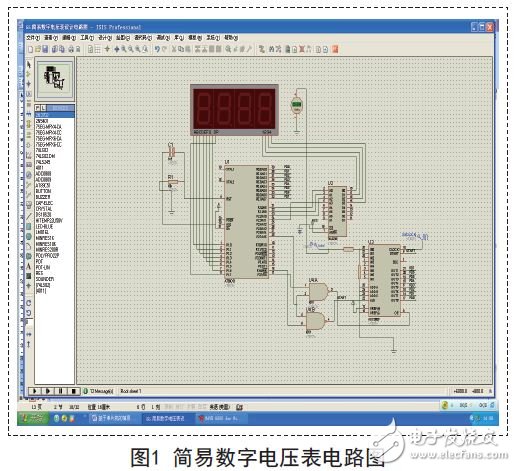
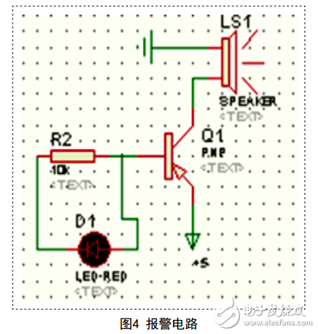
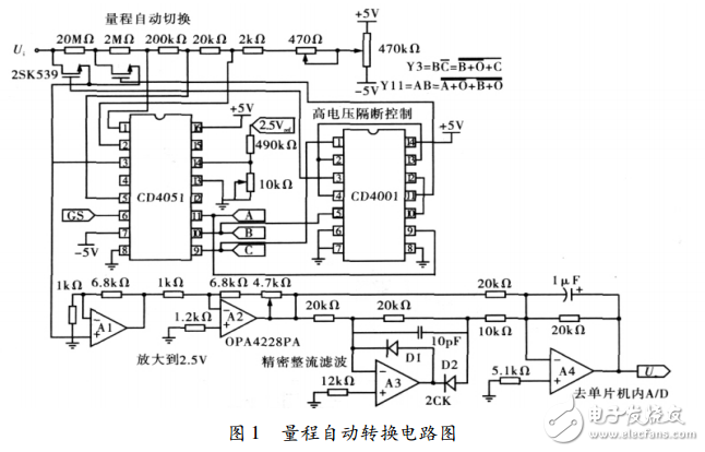
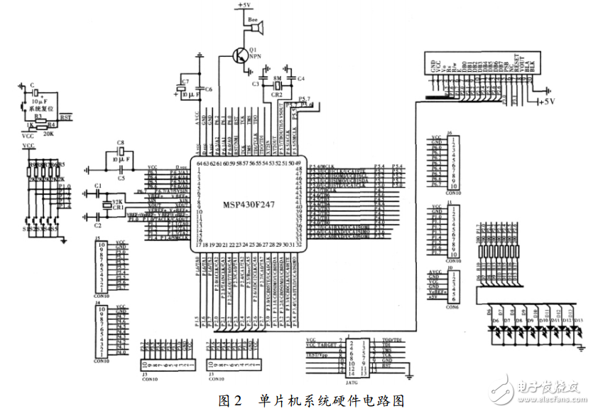
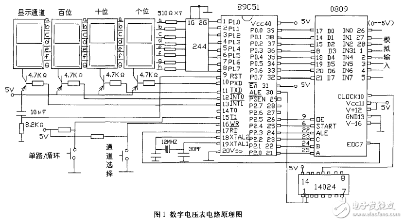


Single-chip digital voltmeter design (nine 51 and MSP430 digital voltmeter circuit schematic)
Design method of single chip digital voltmeter (1) 1. Introduction