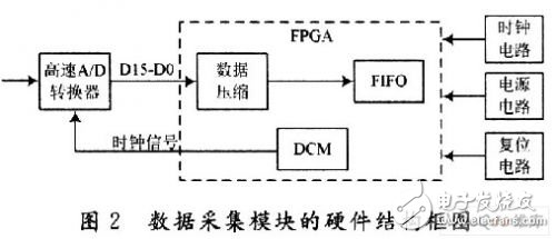
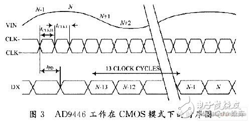
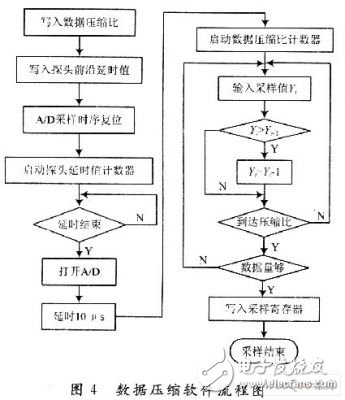
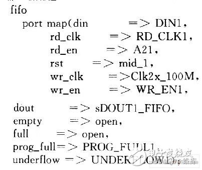
Ultrasound has always been an indispensable technology in the field of medical equipment, with strong penetrating power and high detection sensitivity. However, his current application will no longer be limited to medical care, such as in aerospace, metallurgical and other manufacturing industries. Today, ultrasonic flaw detectors that use ultrasonic non-destructive testing technology are analog and digital. With the development of computer technology, microelectronics technology and digital signal processing technology, traditional analog ultrasonic flaw detectors are gradually being advanced. Replaced by a digital ultrasonic flaw detector. The echo signal of the ultrasonic wave is a high frequency signal, and its center frequency is up to 20 MHz. The frequency of the echo signal in the commonly used ultrasonic probe is generally 2.5 to 10 MHz. To digitize such a high frequency signal, the system is The analog-to-digital conversion circuit places high demands on it. According to the Shannon sampling theorem and the Nyquist sampling criterion, in an ideal data acquisition system, in order to reproduce the input signal without distortion, the sampling frequency is at least twice the highest frequency of the input signal. In actual use, in order to ensure the accuracy of data acquisition, the number of samples in each input signal period should be increased, generally 7 to 10 times per cycle. Some systems have higher requirements for the frequency of the sampled signal. The existing A/D conversion circuit schemes have many shortcomings in reliability, power consumption, sampling speed and accuracy, which cannot meet the needs of some actual situations, and the development of large-scale integrated circuit technology is high-speed, high-precision design. High reliability, low power ultrasound signal acquisition solutions offer the possibility. In this paper, an ultrasonic acquisition module with a sampling rate of 100 MHz is designed, and the sampled data is compressed by the FPGA to buffer the data. Digital ultrasonic flaw detector structure block diagram shown in Figure 1. The digital ultrasonic flaw detector generally includes an ultrasonic transmitting unit, an ultrasonic receiving unit, a signal conditioning unit (including analog signal processing steps such as amplification, detection, filtering, etc.), an analog-to-digital (A/D) conversion unit, a data buffer unit, a data processing unit, and a waveform. Display unit and system control and input/output unit (including communication, keyboard operation, alarm, etc.). This paper mainly discusses the key technologies and implementation methods of high-speed acquisition in digital ultrasonic flaw detectors, involving A/D conversion unit and data buffer unit. 2.1 Block diagram of the data acquisition module Figure 2 shows the hardware block diagram of the data acquisition module of this paper, which consists of high-speed A / D data converter, FPGA, clock circuit, reset circuit and power circuit. Among them, the A/D data converter is responsible for the acquisition and conversion of the analog signal; the FPGA is responsible for acquisition control, data compression and data buffering. The following describes the A/D data converter and FPGA. 2.2 Introduction to AD9446 The AD9446 is a 16 b ADC with a sampling rate of up to 100 MSPS with integrated high performance sample and hold and a reference voltage source. Like most high speed, large dynamic range ADC chips, the AD9446 is also a differential input that provides excellent rejection of even and common mode signals. The AD9446 can operate in CMOS mode and low voltage differential signaling (LVD-S) mode, with mode setting via the output logic control pin. In addition, the digital output of the AD9446 is also optional. Can be direct binary source or twos complement. In the PCB design of the actual circuit, since the AD9446 is a noise-sensitive analog device, the following aspects should be implemented in the specific PCB design: A/D analog power supply separately, analog ground and digital ground single point ground, differential The input lines are of equal length and use an accurate reference voltage source. 2.3 FPGA implementation of acquisition control, data compression and data buffering FPGA mainly realizes the functions of data acquisition control, data compression and data buffering of the entire module. The FPGA uses Xilinx's Spartan3E series (XC3S500E). This FPGA chip is powerful and has a wealth of I/O resources to meet the needs of many practical situations. The following describes the design of data acquisition control, data compression and data buffer FIFO. 2.3.1 Data Acquisition Control The control timing of the AD9446 chip is different from the traditional low-speed A/D. It relies entirely on the clock to control its sampling, conversion, and data output. The AD9446 typically begins sampling conversion on the rising edge of the first clock of CLK and begins to output data after a delay of tpd. The data appears on the D15 to D0 ports only when the 13th clock arrives. Figure 3 is a timing diagram of the AD9446 operating in CMOS mode. The Digital Clock Management Unit (DCM) is a dedicated module for managing and controlling the clock inside the FPGA. It can perform functions such as frequency division, multiplication, debounce, and phase shift. The clock input signal of the AD9446 can be easily controlled by the DCM of the FPGA. In the actual circuit, it should be noted that the clock signal of the DCM multiplier output is matched with the clock input signal of the AD9446. The VHDL language description of the clock output after calling DCM is given below: 2.3.2 Data Compression Data compression processing is one of the important steps in pre-processing the high-frequency sampling of RF signals. It is necessary to compress the sampling data online while maintaining the basic characteristics of the ultrasonic echo signals, and requires the compressed data and the original sampling signal package. The network is consistent. For this reason, in each compression process, only the maximum value obtained by sampling is taken, and other sample values ​​are discarded. The FPGA sends the calculated compression ratio of the sampled data, the probe leading edge delay count value and other data to the corresponding latch, then issues a timing reset command and transmits, starts the probe delay counting, and starts the A/D sampling after the delay. At the same time, the compression ratio counter starts counting. Under the control of the clock signal, each time the sample is sampled, the compression ratio counter is decremented by 1, and the current sample value is compared with the previous sampled value. If it is greater than, the value is saved, otherwise it is discarded until the compression ratio is counted to zero. After that, get a valid sampled data. At the same time, the compression ratio counter is automatically reset and restarts counting. The workflow is shown in Figure 4. 2.3.3 Data buffering In order to solve the problem of rate mismatch between front-end data acquisition and back-end data transmission, a data buffer FIFO is set inside the FPGA, the size is 8K & TImes; 16 b, the compressed data is directly stored in the FIFO, and the microprocessor is FIFO. The reading of the data is completed by the interrupt method. The data buffer FIFO is instantiated by the core generator, and only a small amount of read/write control logic is required to make the FIFO work normally, and the size of the FIFO can be flexibly set within the range of RAM bits provided by the FPGA. The VHDL language description of the instantiated FIFO is given below: The data stored in the FIFO is facilitated by the microprocessor to read, clear, etc. through these logical control ports. The data acquisition module based on AD9446 is designed to realize data acquisition control, data compression and data buffering functions. It simplifies the hardware circuit, improves the reliability and stability of the module, and facilitates the function upgrade of the module. At the same time, the high-speed high-precision analog-to-digital converter is used to meet the requirements of digital ultrasonic flaw detection system for data acquisition accuracy. In addition, FP-GA preprocesses the data, which facilitates the call and post processing of the data by the microprocessor. .
2.0mm (0.079") Pitch Female Headers
Overview
2.00 mm pitch female sockets/headers are low-profile connectors designed for signal and low power PC board connections when space is at a premium. Options include through-hole, surface mount and can be customized for mixed technology, press-fit and pass-through terminations. The pins and blades are available in various sizes, counts, amperages, and plating.
Communications
Through-Hole (Poke-In) 2 Pin Header,2.0Mm Female Pin Header,2.0Mm Pcb Connector,2.0 Pcb Header,0.079" Pitch Female Headers,2.0mm Female Pin Header SMT, 2.0mm Female Pin Header THT ShenZhen Antenk Electronics Co,Ltd , https://www.antenkconn.com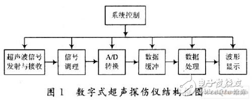

The 2.0mm pitch female headers are commonly found in PC`s and are also made to work in Arduino boards, Arduino Pro and Arduino Mega with either single or double-row female headers, facilitating connections for programming and incorporation into other circuits. They have the perfect height for clearing the USB-B connector and great for stacking multiple shields.
Female header always called as [Header connector", Antenk provide widely range of header connector, from 2.54mm (.100″ inch) pitch to 1.0mm (.039″ inch) pitch. The number of pins (contacts) is from 2 to 40 pins per orw. There are three type: Straight (Dip Vertical), Right angle, SMT (surface mount).
If you can not find the items you interest from above items, welcome to contact us, and you will always get fully responsive from us.
Applications of 2.0mm Pitch Female Headers
Electronics:
LED applications
Arduino boards
Solar applications
Weighing systems
Appliances:
Air conditioner
Refrigerator
Microwave oven
Washing machine
Water heater
Shower toilet
Washer/Dryer
Stove
Automotive, Heavy Duty Military and Marine
For densely packed equipment requiring weight reduction and downsizing and for tough and harsh conditions.
Vehicle infotainment
Computer peripherals
Battery Connections
Battery connections rely on the ability of the current to pass reliable and solid current. This prevents overheating in the circuit and voltage drop.
Rechargeable battery packs
Battery balancers
Battery eliminator circuits
Medical Diagnostic and Monitoring equipment
Heart monitors
Datacoms
Mount Type: Through-hole vs Surface Mount
At one side of this female header is a series of pins which can either be mounted and soldered directly onto the surface of the PCB (SMT) or placed into drilled holes on the PCB (THM).
Best used for high-reliability products that require stronger connections between layers.
Aerospace and military products are most likely to require this type of mounting as these products experience extreme accelerations, collisions, or high temperatures.
Useful in test and prototyping applications that sometimes require manual adjustments and replacements.
2.0mm vertical single row female header, 2.0mm vertical dual row female header, 2.0mm right-angle single row female header and 2.0mm right-angle dual row female header are some examples of Antenk products with through-hole mount type.
Surface-Mount
The most common electronic hardware requirements are SMT.
Essential in PCB design and manufacturing, having improved the quality and performance of PCBs overall.
Cost of processing and handling is reduced.
SMT components can be mounted on both side of the board.
Ability to fit a high number of small components on a PCB has allowed for much denser, higher performing, and smaller PCBs.
2.0mm Right-angle Dual Row female header, 2.0mm SMT Single row female header and 2.0mm SMT Dual row female header are Antenk`s SMT female headers.
Soldering Temperature for 2.0mm Pitch Female Headers
Soldering SMT female connectors can be done at a maximum peak temperature of 260°C for maximum 60 seconds.
Orientation/Pin-Type: Vertical (Straight) and Right-Angle
2.0mm pitch female headers may be further classified into pin orientation as well, such as vertical or straight male header or right-angle female header.
Vertical or Straight Female Header Orientation
One side of the series of pins is connected to PCB board in which the pins can be at a right-angle to the PCB surface (usually called "straight" or [vertical") or.
Right-Angle Female Header Orientation
Parallel to the board's surface (referred to as "right-angle" pins).
Each of these pin-types have different applications that fit with their specific configuration.
PCB Connector Stacking
For 2.0mm pitch female headers, the orientation is either offered as vertical or right-angle, which are options. Elevated sockets/female headers can be available upon request.
Profile Above PCB
This type of configuration is the most common way of connecting board-to-board by a connector. First, the stacking height is calculated from one board to another and measured from the printed circuit board face to its highest insulator point above the PCB.
Elevated Sockets/Female Headers
Elevated Sockets aka Stacked sockets/receptacles or Mezzanine are simply stacked female headers providing an exact distance requirement between PCBs that optimizes electrical reliability and performance between PCB boards.
Choosing this type of stacking configuration promotes the following benefits:
Connector Isolation - the contacts are shrouded preventing cable connection mishaps and good guidance for the mating header connectors.
For off-the-shelf wireless PCB module, stacking height is optimized with elevated sockets.
Offers superior strength and rigidity.
Polarisation prevents users from inverted insertion.
Single, Dual or Multiple Number of Rows
For a 2.0mm straight or vertical female header, the standard number of rows that Antenk offers ranges from 1 to 2 rows. However, customization can be available if 3, 4 or n number of rows is needed by the customer. Also, the number of contacts for the single row is about 2-40 pins while for dual row, the number contacts may vary from 2-80 pins.
Pin Material
The pins of the connector attached to the board have been designed with copper alloy. With customer`s demand the pins can be made gold plated.
Custom 2.0mm Pitch Female Headers
Customizable 2.0 mm pitch female headers are also available, making your manufacturing process way faster as the pins are already inserted in the headers, insulator height is made at the right size and the accurate pin length you require is followed.
Parts are made using semi-automated manufacturing processes that ensure both precision and delicacy in handling the headers before packaging on tape and reel.
Tape and Reel Packaging for SMT Components
Antenk's SMT headers are offered with customizable mating pin lengths, in which each series has multiple number of of circuits, summing up to a thousand individual part number combinations per connector series.
The tape and reel carrier strip ensures that the headers are packaged within accurately sized cavities for its height, width and depth, securing the headers from the environment and maintaining consistent position during transportation.
Antenk also offer a range of custom Tape and reel carrier strip packaging cavities.