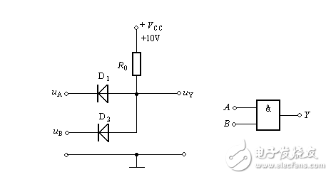
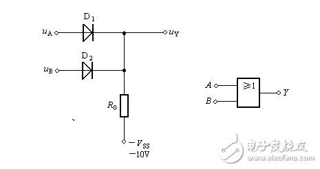
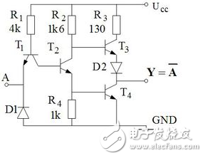
This article introduces the principles of diodes, OR gates, and triodes. As shown in the figure, it is a diode and gate circuit, Vcc=10v. It is assumed that 3v and above represent a high level, and 0.7 and below represent a low level. The following is a detailed analysis based on the situation in the figure: 1. When Ua=Ub=0v, D1 and D2 are positively biased, and both diodes will be turned on. At this time, the Uy point voltage is the diode turn-on voltage, that is, D1, D2 turn-on voltage is 0.7v. 2. When Ua, Ub is high and low, let's assume Ua=3v, Ub=0v. At this time, we may start from D2 and D2 will be turned on. After the turn-on, the D2 voltage drop will be limited to 0.7v. , then D1 will be reversed because the right side is 0.7v and the left side is 3v. Cutoff, so the final Uy is 0.7v, here you can also start from D1 analysis, if D1 is on, then Uy should be 3.7v, At this point D2 will be turned on, then D2 turns on, the voltage drop will change back to 0.7, and the final state Uy is still 0.7v. 3.Va=Vb=3v, this situation is well understood, D1, D2 will be positively biased, Uy is limited to 3.7V. Summarize (by borrowing a definition): usually after the diode is turned on, if its cathode potential is constant, then its anode potential is fixed at a potential 0.7V higher than the cathode; if its anode potential is constant, then The cathode potential was fixed at a potential 0.7 V lower than the anode, and the effect of the diode after the conduction was called a clamp. As shown in the figure, take Vss=0v here, not take -10v 1. When Ua=Ub=0v, D1 and D2 are all closed, then the y point is 0v. 2. When Ua=3v and Ub=0v, D1 is turned on, Uy=3-0.7=2.3v, and D2 is up. Similarly, Ua=0v, Ub=3v, D2 is on, D1 is off, Uy=2.3v. 3. When Ua=Ub=3v, D1 and D2 are all turned on at this time, Uy=3-0.7=2.3v. From the 4kΩ resistor to the “collector junction†of T1, to the emitter junction of T2, and then to the 1kΩ resistor, it is actually a series voltage divider circuit composed of two resistors and two pn junctions. In this loop, the potential is lower. The lower. Therefore, the base potential of T1 is always higher than the collector 0.7V. The forward voltage drop of the pn junction is 0.7V, and the forward voltage drop of the two pn junctions is 1.4V. Then the voltage drop of the two resistors is (5-1.4) V=3.6V, and the voltage drop of the 4kΩ resistor is [4/(4+1). ]&TImes; 3.6V ≈ 2.9V, so the T1 collector voltage is 5-2.9-0.7=1.4V. The water flows to a low place, and the current also flows to a low place. When the A terminal inputs a high level voltage above 3.6V, the 1.4V voltage of the T1 collector is lower than the emitter voltage, and the 4kΩ resistor current flows to the T2 emitter junction through the T1 junction junction, so that T2 is saturated, T4 is saturated, and the circuit outputs a low level. When the A terminal inputs a low level voltage below 1V, the T1 emitter voltage is lower than the collector 1.4V voltage, and the 4kΩ resistor current flows through the T1 emitter junction to the low level input terminal A, T2 cannot get the current and cut off, T4 is cut off, Ucc After R2 saturates T3, the circuit outputs a high level to achieve a non-logical relationship.
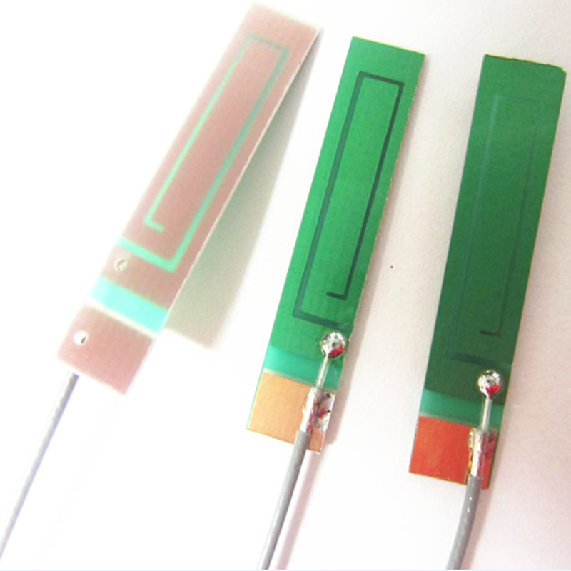
Cellular /WiFi multi-band embedded flexible PCB antenna
It is equivalent to pulling out the antenna line on the PCB board and using other external metals to do the antenna. It is usually used in medium and low end mobile phones with complex frequency band and smart hardware products.
Advantages: suitable for almost all small electronic products, can do more than ten frequency band of complex antennas, good performance, low cost.
The Picture of PCB/FPC/Ceramic Antenna
pcb antenna,5g pcb antenna,lte pcb antenna,lte pcb antenna,2.4g pcb antenna Yetnorson Antenna Co., Ltd. , https://www.yetnorson.com


Disadvantages: need to be debugged separately for each product.
